

Surface defects of optical components
Release time:
2024-06-25
1 Introduction
Surface defects of optical components are often also referred to"Surface Finish" or "Surface Defect", is an index describing the number and size of pitting, scratches and edge breakage allowed on the polished surface. In the imaging optical system, the quality of the component surface directly determines the imaging performance of the system, in the field of strong laser and semiconductor applications, when the component surface quality is not good, it will lead to the situation that the optical system can not be used, therefore, it is very necessary to clarify the definition and determination method of the component surface defect. However, in practice, there are many standards for determining surface defects, and the definitions of each standard are not uniform, which brings some confusion to the actual work of optical practitioners. In view of this situation, this paper from1185-1974Old GB, US Military Standard and ReferenceISO 10110The new national standard three standards, introduce their specific content, as well as the approximate correspondence between each other, so as to help you in the actual work can better identify and control the surface defect index of components.
2 Old GB 1185-1974
In the early days, China's optical industry was relatively weak, and the old national standard used to describe surface defects of optical partsGB/T 1185-1974 "Optical parts surface defects", is in accordance with the Soviet Union's Γ OCT 11141It has been half a century since the standard was revised. There are still many domestic research institutes and arsenals using this standard to define the surface quality of components. Therefore, it is necessary for us to introduce the standard.
In the old national standard, the surface defects were divided10grades, respectively.0,I-10,I-20,I-30,II,III,IV,V,VIandVII, in letters on the drawingBRepresentation. among them,0ToI-30The level is suitable for optical parts located on and near the image plane of the optical system,IIToVIIApplicable to optical parts not located on the image plane of the optical system. The allowable defect sizes and quantities are shown in the following table:
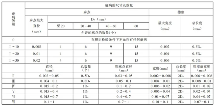
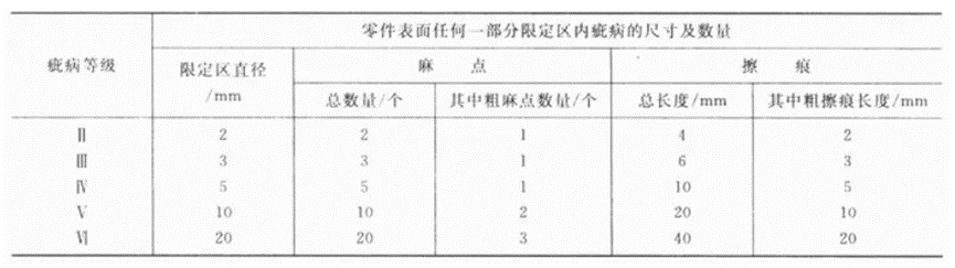
When the size and number of defects on the surface of the part do not exceed the requirements in the above table, but the defects are found to be densely together, the size and number of defects in the limited area shall be specified with reference to the following table, so as to determine the defect level.
This standard mainly depends on the inspector in the approximate.60wunder the incandescent lamp, combined4~10Double magnifying glass for observation, detection when the background is black, so that it is easier to observe the defects of the parts, this method is mostly suitable for transmitted light inspection. Defects that can only be observed under partially reflected light are not easy to be found and need to rely on the inspector's experience and multi-angle observation during the inspection process.
3 US military standard MIL-PRF-13830
American optical designers, usually using1963S. military standards implemented inMIL-0-13830Aor adopt1997Revised inMIL-PRF-13830BAs the basis for the processing requirements of optical components. In the U.S. military standard, two sets of numbers are used to represent surface defects or defect sizes. Usually usedS-DorS/Dsaid,Snamely EnglishScratchThe first letter of the, used to limit the size of the scratch,Also often referred to as the path or Tao,Dnamely EnglishDotthe first letter,Used to limit the size of pockmarks, also known as pits or points. Generally, the ratio of length to width is greater than or equal4:1The defect is regarded as a scratch, and the ratio of length to width is less4:1The defects are regarded as pockmarked.
With regard to scratches and pockmarks, the U.S. military standard is specified in detail as follows:
A, the determination of scratches
The US military standard does not specify the unit of measurement of the scratch, that is, the width and depth of the scratch are not determined, and the actual observation template is used as the standard. The scratch series is the usual scratch number, and the standard sample is10#,20#,40#,60#and80#Total5grade. It is generally believed that the unit of scratch series isμm, Refers to the scratch width, such60#Scratch, which represents the maximum allowable scratch width60μm, I .e.0.06mm. In the US military standard, for non-circular components, the diameter is the diameter of a circle of equal area, and the criteria for determining scratches include5article, as follows:
1、When the number of scratches of the component exceeds the number of scratches required by the surface quality, the component is unqualified.
2、When the scratch level of the component does not exceed the technology required for surface quality, but the component has the largest scratch, the sum of the lengths of all the largest scratches shall not exceed the diameter of the component.1/4.
3、When the component has the largest scratch, and the sum of the lengths of the largest scratches does not exceed1/4For diameter, it is required that the sum of the products obtained by multiplying the scratch length of all grades by the ratio of the scratch length to the diameter of the component shall not exceed half of the maximum scratch grade.
4,When the number of scratch grades of the component does not exceed the number required for surface quality, and the component does not have the maximum scratch, the sum of the products of the scratches of all the grades multiplied by the ratio of the scratch length to the diameter of the component shall not exceed the maximum scratch grade.
5,When the component quality index requires a scratch grade20Or better than this level, the component surface is not allowed to have dense scratches. That is, any diameter in the element6.35mmArea, not allowed to have4Article or4More than or equal10#The scratches.
B, pitting judgment
In the US military standard, the number of pockmarks takes the actual diameter of the allowable defect0.01mmAs a unit of measurement, I .e.50Directly on behalf of the maximum allowed pockmarked0.5mm. If the shape of the pitting is irregular, the average of the maximum length and the minimum width shall be taken as the diameter. The criteria for determining pockmarks include5article, as follows:
1、When the component has a number of pitting stages exceeding the surface quality requirements, the component is unacceptable.
2、Every20mmOnly diameter is allowed1The biggest spot.
3、Every20mmThe sum of the diameters of all pockmarked spots on the diameter shall not exceed the maximum pockmarked spot2Times.
4,When the pitting quality requirement is10or better grade, the distance between any two pockmarked points must be greater1mm.
5,Less2.5μmThe pitting is omitted.
4 with reference to the new national standard ISO 10110
A new national standard for defining surface defectsGB/T 1185-2006, andISO10110-7The provisions for surface defects inISOStandards are based on GermanDIN3140In terms of standard development, therefore, their contents are interlinked.
In the drawings of the new national standard, the relatively complete marking format for surface defects is as follows:
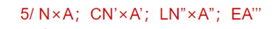
Wherein, No.“5”is the code for surface defects, allowing the degree of defects to be used.N×a.Nfor the maximum number of defects allowed,Ais a series, equivalentmmThe square root of the maximum allowable defect area in units.
When there are requirements for coating stains, useC n' × a'said,CIs the code for the coating stain.N'is the number of the largest stain size,A’For series, the definition is the sameA.
If the length of the pair is greater2mmThere are requirements for long scratches, useL n "×"said,LIt's the code name for a long scratch.N”is the number of long scratches allowed,A"expressed inmmThe maximum allowable width of the scratch for the unit.
broken edgesIt's a''said,EIt's a code name for a broken edge,A”Represents the maximum amount of edge breakage for the edge extension of the component surface, inmmfor the unit.
For example, as shown in the following figure, it includes general defect tolerance, coating defect tolerance, long scratch tolerance and edge breakage tolerance:
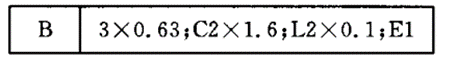
The above drawing requirements indicate that the basic series of general defect tolerance before coating is0.63mm, the allowable quantity is3The basic series of coating layer defect tolerance is.1.6mm, the allowed number is2The basic series of long scratches is0.1mm, the allowable quantity is2Tolerance of edge breakage is1mm.
5 The approximate correspondence between the above three standards
Based on the accumulation of calculations and practical applications, summarize the correspondence between the above three commonly used standards, as shown in the following table:
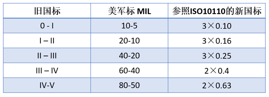
In practice, we can according to the above table, to the standard requirements, so as to find out the customer's demand for surface defect indicators.
6 Conclusion
In this paper, we made a detailed introduction to the criteria for determining the surface defects of optical components, we1185-1974Old GB, US Military Standard and ReferenceISO 10110The basis for determining this indicator in the new national standard. Subsequently, the approximate correspondence of these three commonly used standards is given. Through the introduction of this article, I believe that everyone will have a clearer understanding of the surface finish indicator, and I hope it will be helpful to everyone's work, thank you.
Key words:
Next page:
Recommend News
Changchun International Optoelectronics Expo
2025-06-11
Surface defects of optical components
2024-06-25
Yidexun Optoelectronics Co., Ltd.
Address: Area C, Floor 1, No. 999 Feiyue East Road, Changchun High-tech Industrial Development Zone
WhatsApp:+8613364317271
Contact Phone:+86 13944882736Manager Liu/+86 13944061462Manager Zhao
E-mail:
emily@ydxoptics.com
simon@ydxoptics.com
takukenn@ydxoptics.com


